
General Description:
The DST501 module generates modulated arbitrary frequency chirping CW with frequency update rates up to 250 updates/microsecond (1/8 of the DDS clock rate). The on-board SRAM provides 500K 32-bit word data memory. The DST501 can be controlled by a PC or can work alone with pre-stored chirping waveform. The DDS clock input, DDSCK, can be operated up to 2 GHz with minimum power of 0 dBm. The output of the module consists of a single-ended RF output, OUT, which can be operated anywhere from 5 GHz to 6 GHz.
Key Features:
- 11-bit amplitude and 12-bit phase resolution ROM
- 5 to 6 GHz output frequency range
- High sideband and carrier suppression
- Standard DDS input clock rate at 2.0 GHz for arbitrary chirping
- Optional DDS input clock rate range from 500 MHz to 2.0 GHz
- 500K 32-bit words memory depth with multi-page configuration
- Minimum burst lengths of 256 ns in Triggered Burst Mode
- Up to 2 millisecond chirping waveform at 2 GHz clock rate
- Programmable cyclic length
- Accepts external trigger and generates marker signals (programmable)
- USB 2.0 compliant interface (other interfaces available upon request)
- 18 W power consumption (at 2.0 GHz clock)
- Includes convenient AC wall adapter so no external power supplies are necessary
- User-friendly input data formats and various built-in chirping waveforms
- Companion API and software drivers for easy system development
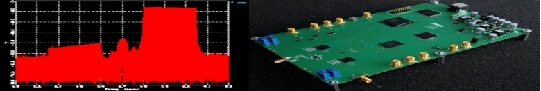
Board Photo:

Detailed Specifications:
| GENERAL | ||
| DDS Frequency Resolution | 32 bits | |
| Frequency Update Rate | 1/8 of Input Clock | |
| Waveform Generation Modes |
Continuous
Triggered Continuous Triggered Burst / Pulse |
|
| User Interface | Windows GUI, USB | |
| DDS INPUT CLOCK | ||
| Type | Single Ended | |
| Termination | 50 Ω | |
| Connector Type | SMA | |
| Frequency Range |
Standard: 2 GHz
Optional: 500 MHz to 2 GHz |
|
| Power Level | 3 to 18 dBm | |
| Return Loss | 13 dB | |
| LO INPUT CLOCK | ||
| Type | Single Ended | |
| Termination | 50 Ω | |
| Connector Type | SMA | |
| Frequency Range | 5.0 to 6.0 GHz | |
| Power Level | 0 dBm to 18 dBm | |
| Return Loss | 10 dB | |
| OUTPUT | ||
| Type | Single Ended | |
| Termination | 50 Ω | |
| Connector Type | SMA | |
| Frequency Range | 5.0 to 6.0 GHz | |
| Output Power | -3 dBm to 0 dBm | |
| Residual Phase Noise @ 10kHz from Carrier | -140 dBc/Hz | |
| Output Return Loss | 8 dB | |
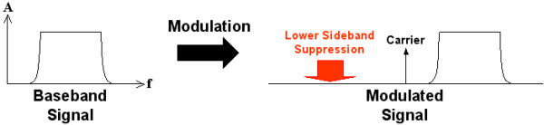
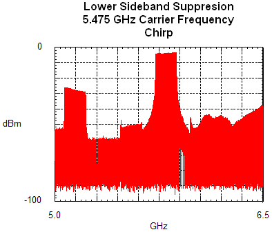
| Carrier Suppression | 35 dB | |
| Sideband Suppresion | 35 dB | |
| WAVEFORMS | ||
| Max Waveform Length | 522,240 frequency words | |
| Max Number of User Pages | 127 | |
| Minimum Waveform Length |
64 frequency words in Continuous or Triggered Continuous modes
256 ns in Triggered Burst mode |
|
| TRIGGER | ||
| Connector Type | SMA | |
| Source | External or Internally Software Generated | |
| External Trigger Threshold Levels |
|
|
| MARKER | ||
| Number of Markers | 1 | |
| Marker Length | User defined | |
| Minimum Marker Length | 4 words | |
| Marker Output Level |
|
|
| API | ||
| Version | Euvis API 2.0 | |
| CLR Language Support |
Visual C++
Visual C# Visual Basic Visual J# |
|
| OPTIONS | ||
|
Variable DDS Input Clock Frequency Range from 500 MHz to 2 GHz
Pre-Stored Linear Chirp Startup Waveform |
||
Functional Overview:
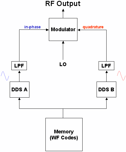
The DST501 consists of two DDS chips to provide the baseband in-phase and quadrature waveforms. DDS A is the left DDS on the board, while DDS B is the right DDS on the board. DDS A is the in-phase input into the modulator, while DDS B is the quadrature input into the modulator. Both the DDS A and DDS B outputs go through a low-pass filter before entering into the modulator. The user will need to provide the carrier frequency, which can be connected to the board using the LO SMA connector.
IQ Select
Although the inputs into the modulator are fixed, either DDS chip can be selected as the in-phase or
quadrature signal. DDS A (left DDS) is connected to the in-phase input of
the modulator, while DDS B (right DDS) is connected to the quadrature input
of the modulator. Depending on which DDS chip is selected as the in-phase signal and which is selected
as the quadrature signal, the modulated output signal from the modulator can either have the lower
sideband suppressed or the upper sideband suppressed.
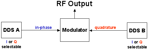
If DDS A is selected as the in-phase signal and DDS B
is selected as quadrature signal then the lower sideband will be suppressed.
Conversely, if DDS A is selected as quadrature signal and
DDS B is selected as the in-phase signal then the upper sideband will be suppressed.
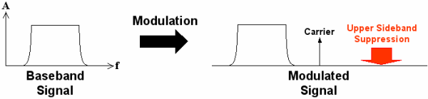
If DDS A and DDS B have the same setting, both are in-phase
signals or both are quadrature signals, then neither sideband will be suppressed.
Spectrum Outputs:
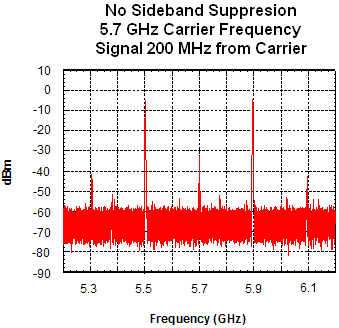
|
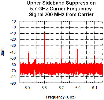
|
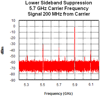
|
|
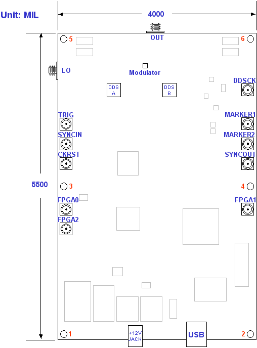
Board Diagram:
Detailed Datasheet:
To get the complete DST501 datasheet, please click here.
Email to: info@euvis.com to get pricing information.